Enhancement Mode of D-MOSFET

Enhancement Mode of D-MOSFET
This figure shows the enhancement mode of operation of N-channel D-MOSFET.Whole construction is similar to the depletion mode of operation of D-MOSFET.But in this enhancement mode of operation of D-MOSFET ,it has no conducting channel .The whole construction acts as capacitor .In this N-channel D-MOSFET ,gate terminal is in positive potential ,it produce negative charges in the N-type conducting channel as shown in above figure .The free electrons drawn in to the N-type conducting channel. by these negative charges.In enhancement mode of operation of the D-MOSFET,free electrons are added in the conducting channel. .As the result amount of the the free electrons are increased in the conducting channel .So N-type conducting channel is enhances or increase .When positive potential on the gate terminal is enhances ( i.e increase) and the amount of the free electrons in the conducting channel is enhanced .From the above discussion we can noted that the amount of the current conduction from the source terminal to the drain terminal through the N-type conducting channel is controlled by the amount of the positive potential on the gate terminal .
When positive potential on the gate terminal is enhances the conductivity of the channel is also enhance .This is the main differences of the D-MOSFET to the JFET .JFET can not be worked in the enhancement mode operation on the opsitive gate termianl.So we can noted that the positive potential on the gate terminal operation is called the enhancement mode of operation of the D-MOSFET.

Depletion Mode of D-MOSFET

Depletion Mode of D-MOSFET
This figure shows the N-channel depletion mode of operation of D-MOSFET.Where the gate terminal is negative potential ,electrons are gather on the gate terminal and protons are gather on the N-type conducting channel (i.e electrons is empty on the N-type conducting channel or depleted) but there are some little free electrons which are responsible for current conduction via N-type conducting channel of D-MOSFET.According to the values of the negative potential on the gate terminal,the resistance of the N-type conducting channel of the D-MOSFET is increase. Consequently ,lesser amount of the free electrons are responsible for the lesser amount current from source terminal to the drain terminal through the N-type conducting channel.From the above discussion, we know that the amount of the current flow from the source terminal to the drain terminal through the N-type conducting channel of the D-MOSFET is controlled by the changing the negative potential on the gate terminal .So the operation is depends on the depleting the N-type conducting channel of free electrons .The negative potential on the gate terminal ,the operation is known as depletion mode of operation of the D-MOSFET.

Operation Mode of D-MOSFET

We know that D-MOSFET can be worked in two mode of operation ,one is depletion mode of operation and another is enhancement mode of operation.Form the construction details of the D-MOSFET we can noted that the whole construction of the D-MOSFET behaves as capacitor where gate terminal of the D-MOSFET acts as one plate of this capacitor and the N-type of conducting channel is acts as another plate of this capacitor .The layer of the metallic oxide (generally the silicon dioxide ) of acts as the dielectric of the capacitor.On the basis of the gate terminal potential the D-MOSFET working mode is classified in two working mode of operation i.e negative potential of the gate terminal operation of the D-MOSFET is called depletion mode of operation and the positive potential of the gate terminal operation of the D-MOSFET is called the enhancement mode of operation.

Symbols of D-MOSFET

D-MOSFET are two types which are following belows;

N-channel D-MOSFET:


Symbols of D-MOSFET


This figure shows the symbol of N-channel D-MOSFET.It consist gate terminal,drain terminal source terminal and sunstrate terminal.In this N-channel D-MOSFET free electrons contributes current flows through the conducting channel from source terminal to drain terminal if the drain terminal is connected positive potential w.r.t source terminal.In N-channel D-MOSFET gate terminal exists like a one plate of capacitor plate and conducting channel exists like another plate of capacitor and oxide layer on the left side of the device acts as dielectric .In this N-channel D-MOSFET gate terminal lead taken out from left side of N-channel D-MOSFET where as drain terminal lead taken out from the top .In the N-channel D-MOSFET the source terminal lead taken out form the bottom of the N-channel D-MOSFET.In this N-channel D-MOSFET the arrow head point to substrate inwards .Hence this symbol is called N-channel D-MOSFET.


P-channel D-MOSFET:


Symbols of D-MOSFET

This figure shows the P-channel D-MOSFET .Just arrow head is different than symbol of N-channel D-MOSFET and all other are same .In this P-channel D-MOSFET tha arrow head is point to outwards of the substrate and holes contributes current in the P-channel D-MOSFET. The conducting channel is made by P-type material and substrate is made by N-type of material and all other construction is similar to that of N-channel D-MOSFET.

E-MOSFET

E-MOSFET
This figure shows the details construction of N-channel E-MOSFET.Gate formation of N-channel E-MOSFET is similar to the N-channel D-MOSFET.This E-MOSFET can be worked in only enhancement mode operation.So this MOSFET is called enhancement MOSFET or E-MOSFET. In this E-MOSFET has no conducting channel between two terminal ,source terminal and gate terminal.Where as in the D-MOSFET has conducting channel between these two terminal,source and gate.We know that substrate of P-type semiconductor material extends one side to another side of the E-MOSFET.But silicon dioxide layer are deposited left side of the E-MOSFET and gate terminal is taken out from this layer .So there is no conducting channel exists.There is needed to form conducting channel or induced channel.To accomplished this task E-MOSFET requires a proper amounts of gate terminal potential (i.e voltage).E-MOSFET have also three terminal, such as gate terminal,source terminal and drain terminal.We noted that E-MOSFET details construction is quite similar to that of the D-MOSFET.Where as there is absence of conducting channel in E-MOSFET.

D-MOSFET

D-MOSFET


It is one type of MOSFET which can be worked in both enhancement mode as well as depletion mode .In the N-channel D-MOSFET it consists of P-type semiconductor material (i.e p-type substrate) on the right side and as well as an insulated gate terminal on the left side of the N-type semiconductor channel .In this type of D-MOSFET here current flowing from source terminal to the drain terminal through the narrow conducting channel between the gate terminal and the P-type semiconductor region or substrate which lies on the right side of the N-type of channel.In the D-MOSFET it has three terminals such as gate terminal ,drain terminal and source terminal.In this type D-MOSFET gate terminal is constructs by thin layer of metal oxide(generally silicon dioxide) is deposited on the left side of the N-type channel pieces. In the D-MOSFET gate terminal is taken out from this deposited metal oxide layer .We know that silicon dioxide is an insulator ,so it like as capacitor where gate terminal act as one plate of capacitor and N-type channel pieces is act as another plate of this capacitor and as well as the silicon dioxide or metallic oxide is act as dielectric .In this type of D-MOSFET gate terminal is insulated from the N-type channel pieces,so we can supply either positive potential or negative potential .As a result D-MOSFET can be worked in both enhancement mode as well as depletion mode where as JFET can be worked in depletion mode only.So D-MOSFET has more advantage than JFET .D-MOSFET have more application in this electronics and communication field.D-MOSFET have also P-channel D-MOSFET which consists a pieces of P-type semiconductor material with N-type semiconductor region (i.e substrate) on the right side and the insulated gate terminal is on the left side of it.

MOSFET

MOSFET means metal oxide semiconductor field effect transistor .MOSFET is same as JFET but some are different .Mode of operation of MOSFET is depletion and enhancement but that of is only one depletion mode in JFET. Commonly used biased circuits of MOSFET is lightly different then JFET For proper operation of the semiconductor devices is that ,the gate terminal of JFET must be in reverse biased connection .IT is the main disadvantage of the JFET(i.eJFET has only one positive gate terminal operation for P-channel JFET where as the only one negative gate terminal operation for N-channel JFET.From above discussion we can note that in JFET only decrease the conducting channel of JFET from its zero bias connection gate terminal size or width of conducting channel because JFET working in depletion mode operation.Hence JFET can worked in only one in depletion mode of operation.But we needed FET also worked enhance(i.e increase ) the size or width of conducting channel of its.Such type of field effect transistor is called MOSFET which has worked in both depletion and enhancement mode.

This type of FET which can be worked in the both depletion and enhancement mode as well is called MOSFET.

MOSFET is a very very important semiconductor devices is the electronics and communication field for many application.MOSFET can be used in any of the FET for corved .MOSFET have many advantages then JFET .MOSFET is more sensitive to change in temperature then JFET .MOSFET have higher input impedance where as JFET input impedance have extremely high input impedance.MOSFET is must useful semiconductor devices.

JFET Applications

JFET has a many applications in electronics and communication field .Some applications of JFET described as following:
JFET buffer amplifier:
It is a one type of amplifier.This JFET amplifier isolates preceding amplification stage from the following amplification stage.A JFET acts as an well buffer amplifier because of the high impedance on output (i.e loading of the preceding stage is high ).This allows the almost whole output from first amplification stage to enter at the buffer input stage.The heavy loads drive by low out put impedance of JFET.This indicates that entire output from the buffer stage reaches the input circuits of the next amplification stage in a JFET buffer amplifier.
JFET phase-shift oscillators:
In the BJT phase-shift oscillators there is appears loading effect because of low input impedance of BJT .To minimise the loading effect in phase-shift oscillators ,the high input impedance of JFET is used in this phase-shift oscillators.
JFET used as RF amplifier:
JFET RF amplifier is used in many electronics and communication field in receiver instead of BJT RF amplifier because of following reasons;
  • JFET has very low noise level.In JFET RF amplifier in receiver JFET will not produces significant value of noise in JFET RF amplifier.
  • JFET is good respond to low current signal generated by the antenna because of JFET is voltage controlled semiconductor devices .SO JFET used as RF amplifier in receiver section in communication or broadcasting field.

JFET

JEFT refer to junction field effect transistor .A bipolar junction has major two disadvantage ,one is low input impedance because of forward biased of transistor and high noise level.To over come those two disadvantage JFET is used in many application instead of BJT.Bipolar junction transistor is a current controlled electronics devices that means the output characteristics of BJT are controlled by input base current where as FET is a electronics devices whose output characteristics of its is controlled by input voltage (i.e electric field).JFET is a one type of FET (i.e field effect transistor).It is used in IC (i.e integrate-circuits) application so it is very very important semiconductor devices in this field. The JFET have three terminal and conduction is done by either electrons or holes charge carriers where as in BJT(i.e bipolar junction transistor ) the current conduction is done by both charge carriers (i.e holes and electrons) .


Symbol of JFET:


N-channel JFETP-channel JFET

Construction of JFET:


This figure shows the construction of N-channel JFET .Here is only one type (i.e n-type ) semiconductor material is used as bar with two PN junction layer at the side of the this bar as shown in figure below.Conducting channel for the charge carriers is formed by the bar material . At the side of the bar material P-type material is diffused in proper amount if the bar is N-type material .If this conducting channel is N-type s/c material and diffused material is P-type then this type of JFET is called N-channel JFET where as If the conducting channel is P-type material and diffused material is N-type then this type of JFET is called P-channel JFET.


construction of JFET
This above figure is N-channel JFET. In this construction two PN junction forms such as two diodes connection internally at the side of the bar.The terminal which is taken out from diffused material is called Gate terminal (G). And other two terminal which are taken out from Bar material is called Drain terminal (D) and source terminal (S).So JFET has three terminals such as gate ,drain and source terminals.

Polarities of JFET:

polarities of JFET

This above figure shows the general polaritie

s of N-channel JFET where as the polarities of P-channel JFET is just opposite is that of N-channel JFET.
JFET is three terminal electronics devices. It consists of Gate terminal ,Drain terminal and Source terminal .In put gate voltage or potential between the gate terminal and the source terminal is always reverse biased in the both type of the JFET and source terminal is such that way internal PN junction diode becomes reverse biased connection .That why JFET has high input impedance .The drain terminal and source terminal can interchange But one things can be always take care that the drain terminal is so c

onnected w.r.t source that the drain current is always flows from source terminal to the drain terminal and the amount of source current is equal to the drain current.


Principle of JFET:


This JFET circuit shows N-channel JFET with general polarities where gate input voltage is reverse bias with source.In this JFET circuit the two depletion layers are formed at the side of two PN junction in its internal body .This is N-channel JFET circuits so current conduction is

done by free electrons where as in the case of P-channel JFET circuits polarities is just opposite that of N-channel JFET circuits and current conduction is done by hole charge carriers . In the case of fixed width of conduction channel its resistance can be controlled by varying input gate voltage or potential. If the reverse input gate voltage is high the area of depletion layers is increase and conducting channel is decrease .Hence drain current is decrease .So conducting channel is varied by changing the reverse input gate voltage (i.e amount of drain current can be change according to input gate voltage .


Working of JFET:It has two condition as below:

  • When Gate voltage is zero :
When the input of the biased is open (i.e potential deference between the drain and source terminal is zero or gate voltage is zero as shown in figure below .The depletion layers is form at the side of the bar by the two PN junction .Under this condition current conduction from source to drain via conduction channel between two depletion layers determine the width of the conducting channel and amount of current flow.

working of JFET


  • When gate voltage is applied:
Connection of the gate terminal and source terminal is reverse biased .If the input voltage is applied or closed to gate and source terminal then the width of the depletion layers is increased .Hence the width of the conducting channel is decreased and resistance of N-type conducting channel bar is increased .As a result flow of current from source terminal to the drain terminal is decrease because of its resistance .Just opposite action will happen if input gate or reverse voltage is decrease .Hence the drain current is increased because of its resistance decrease.Hence it is note that flow of current from source to drain can be controlled by reveres gate input voltage .This is similar way , in the case of P-channel JFET but current conduction is done by holes instead of electrons in N-channel JFET and polarities is just opposite that of N-channel JFET.

Features of JFET: JFET has following features;

  • In JFET gate-source PN junction of JFET is always worked in reverse biased connection.
  • JFET is voltage controlled semiconductor devices with three terminals (i.e gate ,drain and source termianl)
  • In JFET the output drin current is controlled by varying the width of the conducting channel.
  • Gate current in JFET is zero.
  • Since in JFET drain current is equal to the source current at that condition.
  • JFET is not temperature sensitive devices.
  • In JFET depletion layers of Pn junction increase or decrease by an equal amount because of same potential in two input gate terminals.
  • JFET is working in two conditions that is when gate termianl voltage is zero and when gate terminal voltage is applied.

Advantages of JFET:

BJT is current controlled devices where as JFET is not current controlled devices but JFET is voltage-controlled semiconductor devices (i.e change in input voltage controlled the output drain current) .JFET is similar to a vacumm pentode but it has more advantages;

  • In JFET input impedance of its is very high.
  • It has high isolation between input circuits and output circuits.
  • JFET is negative temperature co-efficient of resistance devices.
  • JFET has no risk of thermal runway.
  • JFET has long life.
  • JFET has high efficiency .
  • JFET is smaller in size.
  • Power gain of JFET is very high ,Hence no needed of other amplifier stage.

JFET Amplifier

JFET amplifier

Here given figure shows JFET amplifier circuits of one stage .It consist of biasing voltage JFET ,coupling devices such as capacitor in out put circuits . The weak input signal which can be going to be amplified is given between gate terminal and sources terminal with the help of the reverse biasing voltage between these two gate terminal and source terminal .Amplified output signal is obtained in the output drain-source terminal circuits .For proper function of JFET we must take care in polarities of JFET and biasing voltage .Here input gate terminal must be negative w.r.t source terminal in every JFET amplifier (i.e input circuits always be reverse biased in every JFET amplifier ). It consist of extra biasing circuits So for this biasing voltage battery is connected in this JFET amplifier.
In this case small change in the reverse input biasing voltage produces a large change in drain current in output circuits of JFET amplifier.Hence JFET act as amplifier which amplified a weak input signal.

At the time of positive half-cycle of input weak signal the reverse biasing voltage on the gate terminal decreased .hence the width of the conducting channel is increased and also increased drain current in the JFET amplifier.

At the time of negative half-cycle of input weak signal the reverse biasing voltage on the gate terminal is increased .Hence the width of the conducting channel is decreased or become narrow and decreased drain current in the out put circuits of JFET amplifier.It is noted that a small change in input gate voltage at the gate terminal produces a large change in drain current at the output of JFET amplifier .So JFET act as an amplifier .

Connection of JFET amplifier:

JFET has a three terminal such as gate ,drain and source terminals But when JFET are going to be connected in JFET amplifier circuits it has needed four terminals.Two terminal for input circuits and two terminal for output circuits connection.But here one terminal is common both input circuits and output circuits .So following are the JFET amplifier connections :

  • Common drain connection JFET amplifier circuits
  • Common source connection JFET amplifier circuits
  • Common gate connection JFET amplifier circuits


But from above connection JFET amplifier circuits the common source connection JFET amplifier circuits is must extremely used connection as JFET amplifier because of its high input impedance ,moderate output impedance and well voltage gain .But this JFET amplifier connection provides phase reversal (i.e the angle of output signal is 180 degree difference compare with the angle of input signal).JFET amplifier in common source connection JFET amplifier circuits is similar with the common emitter transistor amplifier.


JFET amplifier(practical):

JFET amplifier

JFET amplifier accomplished faithfull amplification when associated circuits used or connects properly with JFET.Above JFET amplifier shows the practical JFET amplifier which consists of following components properly as shown in above figure.


  • Gate resistor(R2) : In JFET amplifier gate resistor is used to maintain gate terminal is nearly about 0 V d.c (i.e gate terminal current is approximately zero).Gate resistor is in several mega ohms value which prevents loading of the a.c signal source.

  • Coupling capacitor(C1) : In JFET amplifier coupling capacitor used as coupling devices to one stage to next stage and in input gate terminal in order to pass only input a.c signal and blocked d.c biasing signal .

  • Bypass capacitor(Cs) : In JFET amplifier it is used with source resistor in parallel as shown in above figure.Which provides easy path for a.c signal to grounded which prevent voltage drop in source resistor and increase voltage gain.


Rectifier (using diode)

In electronics device rectifier are widely used in power section .It is used to rectified alternative current(ac) into direct current(dc) this process is known as rectification .In this device, diode capacitor ,inductor ,resister is widely used.Rectifier also make with the help of vacuum tube
diodes,mercury arc values and other components
If we wants to convert direct current(dc) into alternative current(ac) this device is known as inverter.
The type of rectifier are determine by the number of diode used in specific arrangement of diode There are following type of rectifiers which are only the uses of diode :
  1. half- wave rectifier
  2. full-wave rectifier
  3. bridge rectifier


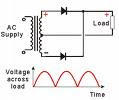
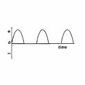
In the half-wave rectifier ,only one either positive part or negative part of AC wave is passed.It is depends upon the uses of diode in positive half of transformer or negative half of transformer in series .It is very inefficient ,because only one half signal is reaches in output section of it .Half-wave rectification is achieved with the help of three diode in three-phase system and with the help of one diode in one phase system.
The output of DC voltage of half of rectifier can be calculated by followings theoretical equations.

  1. Vpeak=Vrms*1.1414
  2. Vdc=Vpeak/3.14


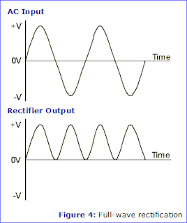
In the Full-wave rectifier,full waveform of AC wave is passed to output section.In this rectifier whole part of wave form are achieved in out put so this is more efficient than half wave rectifier.Four diode are used in full wave rectifier circuit if there is non-center trapped transformer is includes.Two diode are used in full-wave rectifier circuit if there is center-trap transformer is includes.


Half-Wave Rectifier:


According to the diode action ,the rectifier conducts signal (i.e current) only at the time of positive half cycle of input a.c signal where as the negative half-cycle of a.c signal are cutoff or suppressed. At the time of negative half-cycle ,no current conduct in the circuits.Therefore no voltage drop across the lad resistor.That's why,signal (i.e current ) always flows in only one direction (i.e d.c signal) via the load resistor after every half-cycles.


Circuits Explains:


half-wave rectifieroutput of half-wave rectifier


It consists of one diode ,transformer and load with complete close circuits.So this single S/C diode acts as a half-wave rectifier.The a.c signal which is going to rectified is applied in series with the signal diode and load resistance as shown in above.Usually ,a.c supply is applied via a transformer .By the transformer action ,It has two advantages ,one is it allows at step up or step down the a.c input signal as our desire and other is it isolates the rectifier circuits form power line and therefore it decrease the risk of electric shuck in the circuits or equipments.


Working Explain:


The applied a.c signal across the secondary winding change polarities after each half -cycle of supply a.c voltage.At the time of the positive half-cycle of supply a.c voltage,upper end of secondary windings becomes positive w.r.t the lower end of its.In this condition diode is in forward biased and it conduct current in the circuits.At the time of negative half-cycle of in put a.c voltage ,upper end of secondary windings is negative w.r.t the lower end of its.In this condition ,diode becomes reverse biased and it does not conduct current in the circuits.In this way, current flows via the load at the time of positive half-cycle of input a.c voltage only where as no conduct current through the load at the time of negative half-cycle of supplied a.c voltage in the same direction is obtain across load for other next cycle.But this output is pulsating d.c .Hence to reduce it an extra filter circuits is used .


Limitations:

  • The output is low because a.c supply delivers power only half-cycle time
  • To remove pulsating d.c it required extra filter circuits .


Full-Wave Rectifier:


In this full-wave rectification,two diode are used in such way that they work alternately.Current flows via the same direction at the time of both half-cycle of input a.c voltage .During the positive half-cycle of input a.c voltage one diode conduct current through the load and during the negative half-cycle of the input a.c voltage ,next one diode conducts current via load in same direction.In this way full-wave rectifier circuits utilises the both half-cycle of input a.c voltage to produce the d.c output .Therefore its efficiency is higher than half-wave rectifier.


Center-Tap Full-wave Rectifier:

Circuits details:
It consists of two diode ,one center-tapped transformer and load with the power supply in closed circuits as shown in figure below.Secondary winding of center-tap transformer is used with those two diode s connected in such way that each diode use s one half-cycle of input a.c voltage. That means upper diode use to conduct the upper half-cycle of secondary winding whereas lower diode is use the lower half-cycle of secondary windings.

center-tap full-wave rectifier

Working Explains:

At the time of positive half-cycle of secondary winding voltage ,the upper end of secondary winding becomes positive w.r.t the lower end of its.Under this condition ,upper diode is in forward biased whereas lower diode is in reverse biased.Hence upper diode conduct positive half-cycle of the input of the a.c voltage where as lower diode does not conducts.At the time of negative half-cycle of secondary winding ,upper end of secondary winding become negative w.r.t the lower end of its.Under this condition ,lower diode is in forward biased where as upper diode is in reverse biased.Hence the lower diode conduct current via load of the negative half-cycle of input a.c voltage and upper diode does not conducts current .The current in the load is in same direction for both half-cycle of input a.c voltage.In this way d.c output is obtain across the load .

Limitations:

  • It is difficult to locate exact the center tap on the secondary winding of transformer.
  • The diode used must have large peak inverse voltage.
  • Each diode utilises only one half-cycle of secondary voltage,so the d.c output is small.
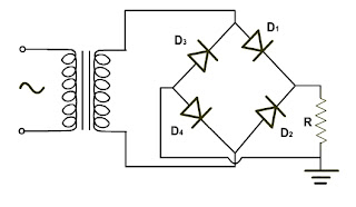
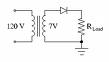
Full-Wave Bridge Rectifier:

It consists of four diode ,transformer and load resistor connected as shown in figure below .The a.c signal is applied to the diagonally opposite ends of the two diode whereas another two ends of the diode is connected to the load resistor as shown in figure.

Operation details:


At the time of positive half-cycle of secondary winding voltage the upper end of the secondary winding becomes positive w.r.t the lower end of its.Under this condition diode D1 and D4 are in forward biased where as other diode are in reverse biased .Hence the diode D1 and D4 conduct current through the load resistor.

At the time of negative half -cycle of the secondary winding voltage ,the lower end of the secondary winding is positive w.r.t the upper end of the secondary winding .Under this condition , D2 and D3 are in forward biased and where as other diode are in reverse biased .Hence the diode D2 and D3 conduct current through the load resistor .This flows of current is in same direction as for positive half -cycle of the secondary winding voltage .Hence d.c output is obtain across load resistor.

Full-wave bridge rectifieroutput of Bridge rectifier

Advantages:
  • No required of center-tap transformer
  • For the same secondary winding voltage the output is twice that of center-tap full wave rectifier circuit.
  • For same d.c output ,the PIV is one-half of that of center tap full wave rectifier.
Limitations:
  • Four diode are need for this circuit.
  • The voltage drop in the internal resistance is twice as in the center tap full wave rectifier circuits because of four diode.

S/C diode as Rectifier


S/C diode has a wide range of application ,one of them is rectification.The diode is used in rectifier circuits to rectified a.c input signal .Here diode and load resistor (RL) are connected in series as given below.The rectified signal (i.e d.c output) is obtained across the load resistor.
diode as rectifierout put of diode


Circuit details:

Diode conduct current in forward biased or one direction.So at the time of positive half-cycle of a.c input signal ,the S/C diode conducts this signal in the circuits because of forward bias .As a result the positive half-cycle of input signal appears across the load resistor as shown in figure below.But at the time of negative half-cycle of input a.c signal ,diode does not conduct current because of reverse biased.As a result no voltage appears across the load resistor .In this type of circuits the negative half-cycle are suppressed

but output consist of only positive half-cycle of in put a.c signal.In this way ,S/C diode act as rectifier (i.e a.c input signal changes into d.c out put).


amp circuit

Multi-Stage Transistor amp circuit:


In the field of amp circuit ,one stage in not capable to amplifying weak signal to required strength or level .Therefore multi-stage amp circuit is necessary to amplifying up to desire level signal stage amp circuit is generally insufficient to drive or run at output of electronics equipments .Therefore an extra amplification is necessary .For this other level or stage is needed .In order to accomplished this ,the output of one stage amp circuit stage is coupled to another or next input of amp circuit .The whole construction of this amp circuit is Multi-stage amp circuit.It has wide range of application in this field .For example ,Radio communication system , number of amplification stage may be greater than five stages.


According to coupling devices amp circuit are classified as followings;

  • Direct-coupled amp circuit :In the case of direct coupling (i.e d.c coupling the one stage of the amp circuit are directly connected to another stage of amp circuit without d.c isolation.This type of amplifier widely used in the low frequency (i.e less than 10Hz) signal to be amplified .For example ,amplifying thermo-couple current ,photo-electric current etc.There is no coupling devices (such as capacitor ,transformer etc) because at low frequency the electrical size of these elements become large .Therefor output of one stage is directly connected to the input of the next stage of an amp circuits with out coupling devices.

Circuits Details:

There are two stage direct-coupled amp circuit.It consists of two NPN transistor and next so on It is very simple amp circuit .The first transistor output from collector is connected to the input of the next stage of the transistor base .And similar way for the other additional stage .This circuits is stable even temperature is change .

The weak a.c signal is given to the base of the first transistor .The amplified a.c signal appears across the output or collector of the same transistor .This amplified a.c signal is also give to the base of the next transistor of further amplification and amplified a.c signal is appears across the collector load or out put of the same transistor . For other additional stage similar way ,this type of amp circuit amplified the weak signal which is less than 10Hz.

direct-coupled transistor amplifier

Advantage :

  • The construction of this type of amp circuit is very simple.
  • It contains minimum number of resistor.
  • This amplifier circuits does not contains coupling devices .So it has low cost .

Limitations:

  • This amp circuit can not be used at high frequency (i.e greater than 10Hz) for amplification.
  • Because of temperature change ,the operating point of amp circuit is shifted.


  1. RC-coupled amp circuit : A capacitor is used as the coupling devices ,in the RC -coupled amp circuit of electronics equipment.Here capacitor connects the output of the first stage of amp circui to the input of the an next stage of amp circuit.By the same way for other required stage.Here the capacitor is used allow to pass the a.c signal where as block the d.c biasing voltages.This type of circuits is most useful circuits.It is simple in construction.and it has low cast .It give well audio fidelity over wide rage of frequency.Capacitor is used as coupling device which connect the output of the first stage of transistor to the next stage input base of next stage of other transistor in amp circuit and soon for other stage.This type of amp circuit is generally employed for voltage amplification.
Circuits details:

RC-coupled transistor amplifierpower gain
Here weak a.c signal is given to the input base of the first transistor .Amplified a.c signal is appears across its collector resistor or load (Rc).This amplified a.c signal is also given to the input base of the next transistor for further amplification with the help of coupling capacitor .This amplified a.c signal is appears across the collector load (Rc).This stage does further amplification of the applied a.c signal.In this same way ,cascaded (i.e one stage after another stage) stage s amplify the a.c signal and as a result overall gain of amp circuits is increase .But here total gain of the amp circuit is less than the gain of the individual stages because output of first stage drives the second stage and soon .Due to the shouting effect of the input resistance of second stage of the amp circuit ,the effective load resistance of first stage of amp circuit is reduced. But in the case of 3-stage amplifier circuits total gain of the amp circuit is equal to the product of the individual stage of amp circuit .

Advantages:

  • It contains the resistors and capacitors as coupling devices .So it has lower cost .
  • It provided excellent audio fidelity over wide range of frequency.So it has excellent frequency response.
  • This amp circuits is easy to make and compact.
Limitations:
  • This type of amplifier has low voltages gain and as well as power gain.
  • It has noise in the circuits with age.
  • It has poor impedance matching.

Transformer-coupled amp circuit :A transformer is used as coupling devices in transformer coupled amp circuit .It also allow to pass the a.c signal whereas block the d.c signal .In this circuits additional impedance matching circuits is necessary.The main disadvantage of RC-coupled amplifier is low voltage or power gain .This is over come by this transformer-coupled amplifier circuits.In RC-coupled amp circuit ,effective load resistance (Rc) of each individual stage is decrease because of low resistance presented by input of each individual amplifier stage and previous stage .That means impedance of input of an amplifier is low whereas its output impedance is large.In the case of multi-stage amp circuit ,the large output impedance of one stage of an amplifier circuits become in parallel with the low input impedance of next other stage.Therefore effective load resistance is decreased.Transformer has a properties of impedance change with the frequency ,the low impedance of a one stage of amplifier circuits load can be reflected as high load impedance to the preceding stage of an amplifier circuits.This type of amplifier is generally employed when the load resistance or impedance is small.RC coupled amplifier is used for voltage amplification whereas Transformer-coupled amplifier is used for power amplification.

Circuits details:

This figure shows two amplification stage of transformer coupled amp circuits .Here transformer is used as coupling devices which connect the output of one stage to the input of next amplification stage of amp circuit. In this type of amplifier circuits primary coil of this transformer is made the collector load where as secondary coil is connects as input to the next stage.

Transformer-coupled amplifier

In this amp circuit an weak a.c signal is given to the input base of first transistor ,amplified a.c signal is appears across primary coil of the coupling transformer .By transformer action, the voltage is developed across primary coil is transferred to the input of the next of next transistor by the secondary coil of transformer,amplified a.c signal is shown by similar way across the next collector load or resistor.

Advantages:

  • In this amplifier circuits ,no a.c signal power is lost in base resistor or collector.
  • It provides an excellent impedance matching due to transformer-coupled.
  • It provides higher voltage and power gain.

Limitations:

  • It is bulky and fairly expansive at audio frequency.
  • The gain is change considerably with frequency .So it has a poor frequency response.
  • It has high frequency distortion.
  • This amp circuit tends to introduce hum in the output stage.

amp circuit

Introduction :
In almost all electronics equipments contains amp circuit. In this type of equipments ,there is necessary to rise or increase strength or level of signal which is weak.The importance of amp circuit is very very much in this field .So we can say that it has wide range of application .Amp circuit are used in order to amplifying weak electrical signals.
The transistor are widely used in many places such as scientific ,medical ,communication field etc to produced signal in the micro volt and Milli volt range which is weak level signal .So it should be necessary to increase its level or strength using amp circuit drive required equipments .Amp circuit are classified according to their uses or ranges like below:
  • Pre-amp circuit ,
  • Voltage-amp circuit and
  • Power-amp circuit.

Before the invention of transistor ,vacuum tube ,Mercury arc values etc are used in amp circuit .But now transistor is mostly used in amp circuit.According to the number or stage of transistor used in amp circuit ,it is classified as below:

  • Single-stage transistor amp circuit and
  • Multi-stage transistor amp circuit .

How amp circuit amplifies?

Now we are discussed about transistor amplifying or analysis of amp circuit.This type of configuration is called common emitter configuration.

amp circuitsgraph of amp circuits


This type of amp circuit consists of transistor and its biasing resistors ,which help to amplified the weak a.c signal in sufficient level or strength at the out put of the amp circuit. When weak base a.c signal is given to the base of the transistor as above figure ,then the very large voltage(i.e Bita times or 100 times the base currents) appears across the collector resistor( Ro) ,because of high value of collector resister .So we get very large output voltage .This way the transistor amplifies weak signal.

Practical amp circuit:

This amp circuit is a practical circuits .For the required amplification of weak signal ,various circuits elements and their working principle in the amp circuit .Some important terms of practical amp circuit which are described as following:

amp circuits

Input capacitor(Cin):The practical amp circuit consist of an electrolytic capacitor at the input of the each stage which is connected in base of the each transistor in the case of transistor amp circuit .This is used to allows to pass the a.c signal through it whereas block the d.c biasing signal .

Biasing Resistance circuits :It consists of three resistor (i.e Rb1,Rb2 and RE) which are used to proper biasing and stabilisation circuits .This circuits maintain the proper operating point .If the biasing circuits of amp circuit should not be proper arrangement some portion of the negative-cycle of input signal may be cut off in the collector load or out put .

Coupling capacitor(Cc) :This capacitor is used to couple one stage of amp circuit to the next stage of amp circuit .According to the capacitor function ,it isolates the d.c biasing signal of one stage of amp circuit of the next of amp circuit , But only allows to pass the a.c signal which is applied for amplification . If it is not used in amp circuit whole biasing function is unbalanced due to shouting effect of collector resistor.

Emitter by pass capacitor(CE):This capacitor is used in emitter side for grounded it .It is used in parallel with emitter resistor and provided a low resistance path or way, to the high frequency signal or amplified a.c signal .The amplified signal is flowing via collector resistor (Rc) as a result voltage drop across it which reduce the output voltage ,i f we not used it in amp circuit.

Requirements of faithful amplification

The system of increasing the strength or level of weak signal in a circuit without any changes into its waveform is called faithful amplification.
The principles of transistor reveals that it will work correctly if its emitter-base junction (i.e input circuit) connected in forward biased and the collector-base junction(i.e output circuit ) connected in reverse biased at the all times.To achieving faithful amplification , this is main key factor. To achieve this ,the followings general conditions must be satisfied:
  1. Proper amount of zero signal collector current
  2. Minimum amount of proper base-emitter voltage at any times
  3. Minimum amount of proper collector-base voltage at any times

The first and second conditions shows that base-emitter junction shall connected correctly in forward biased in the circuit at the all times and the third condition shows that base-collector shall connected correctly in reverse biased in the circuit at the all times.

To fulfil of these condition transistor work between saturation to cutoff region i.e active region.

Classification of transistor amp circuit

Basic tr amplifier
Transistor amplifier
There are many applications of transistor in the electronics and communication field.Manly it is used in amplification purpose in the circuits.They are classified according to their uses ,frequency capabilities, coupling devices and mode of operations which are as following:
  1. According to use; transistor amplifier are classified as voltage amplifiers and power amplifiers.At first it is use to increases the voltage level or strength of the signal while the after it increase the power level or strength of the signal in the circuit.
  2. According to the frequency capabilities; these are classified as audio amplifiers ,RF amplifiers etc which are use to amplify the lying in the audio range (i.e 20Hz -20kHz) and radio frequency range etc respectively in the circuit.
  3. According to coupling devices; if there is a single stage amplifier, it is unable to amplify the signal to fulfill the practical requirements.So other additional amplifier i s necessary to amplify the signal.But to preform this of the one stage is required to coupling to the other next stage.So depending upon the coupling devices used in the circuit,the transistor amplifier are classified as direct-couple amplifier,R-C couple amplifiers, transformer couple amplifiers etc.
  4. According to the mode of operation; the transistor amplifiers are classified as class-A amplifiers,class-B amplifiers, class-C amplifiers .This classification in depends upon the portions of the input waveform which reached into output stage. For more

Electro-mechanical switch or Relay

Introduction:
It is a mechanical switch but it preform electrically switching operation (i.e turn ON or OF current ) in an electronics or electrical circuit.


figelectro-mechanical switchsimple fig

This type of switch is devanced or improved form of mechanical switch .In general type of Relay it consist of a solenoid and leaver carring with armature .Those are suspended on the constant body with the help of the spring .When solenoid enerasised it pulls lever downwards and vice-versa .Solenoid consist of extra power supply with the switch .When the switch of the solenoid is closed ,the armature is closed the relay contacts (i.e turn On or closed circuit). When the switch of the solenoid is open ,then the armature contacts of the relay is open (i.e turn OFF or open circuits).In this way this type of the switch is preform the switching operation .

Advantages:
Following are the advantages of the electro-mecanical switch over mecahnical switch;
This type of switch need a small power to perform its switching peration .This type switch handel large power.
  1. It has no risk of sparkings durings switching operation.
  2. This can perform switching operation from a distance .So it can handeled high voltages.
  3. In this type of switch relay current is smaller than load current.

Limitations:

* The speed of switching operation is very small.
* Littel wear and tear is possible because of moving parts.


Electronics Switch

Electronics Switch
This type of switch preform switching operation (i.e ON or OFF current) in an electronics or electrical circuit with the help of electronics components such as transistor ,tubes etc. It has many advantages and popular because of their high speed of switching operation and no sparking in the circuit..Transistor ,SCR, Tubes etc are used as a switch.In the case of transistor switch, it operates at saturation region or at cut off region.
  • The transistor is cut off region or no cur5rent flows in collector load , when input base voltage is proper amount of negative potential .At this condition ,there is no voltages drop across the collector resistor or load and the out put voltage is theoretically Vcc.

Therefore,

Ic=0 and

Vce=Vcc

This condition shows that ,it is open circuit (i.e OFF state).

  • The transistor is in saturation region or current flows in collector resister or load, when base input voltage is proper amount of positive potential. In this condition, almost whole voltage(Vcc) will dropped across collector resister or load and out put voltage is theoretically zero.

Therefore,

Ic=Isat and VCE=0

This condition shows that ,it is a closed circuit (i.e ON state).

Advantages:

This type of switch have following advantage than other type of switch:

  1. It preform noiseless switching operation because of no moving parts in this type of switch.
  2. The size and weight of its is smaller than other.
  3. It has easy to maintenance .
  4. It has lower cost than other.
  5. It has very fast speed of switching operation than other type of switch.
  6. It give well services (i.e trouble free) than other.

Mechanical switch

Mechanical switch
This type of switch operated mechanically to preform turn ON or OFF current in an electronics or electrical circuits is called a mechanical switch .This type of switch perform switching function with some sparking. So it has low efficiency than other .
The tumbler switch is c one of the example of a mechanical switch which is used in many home appliances to perform turn ON or OFF power supply such as bulbs , heater , fans etc .In mechanical switch ,load is connected in series with a mechanical switch and the power supply (i.e battery).When the switch is close ,there is current flows in the circuits (i.e through load).When switch is open ,then there is no current flows in the circuits (i.e via load).

Disadvantages Of Mechanical Switch.
  1. In the close circuits ,the switch carries whole load current.When if there is high load currents,the contacts of switch enable to carry it without overheating.So the size of the switch is increase accordions to amounts of load current.
  2. The speed of switching operation is very low ,because of its high inertia.
  3. When the load current is high in the circuit ,then the sparking is possible at the contacts of the switch at the time of switching operations(i.e ON or OFF).

Solid-State switching Circuits

solid-state switch
Introduction:
In many operations,there is required to switch on (i.e close circuit ) or switch off (i.e open circuit) in electrical circuits or electronics circuits .In some high sensitives applications it is necessary that to switch ON or switch OFF should be very fast and but not sparking in the circuits.Because of these two major reasons , the mechanical switches can not be used in the circuits for the switching purpose .This type of switch has high inertia.Therefore its speed of operations is low.This type of switches has sparking properties at the time of conduction of switching operations.
In this fast and movable world ,very high speed of switching operations without any sparking switching devices is needed.For this purpose tube and transistor are used in the switching circuits to accomplished switching operations .Such type of switches are called electronics switches .The electronics switches are also widely used to generates non-sinusoidal wave (i.e square wave , triangular wave or saw-tooth wave ,rectangular wave).
A circuits which ,preform turn ON or turn OFF current in an electronics or electrical circuits is called a switching circuits.Actually this circuit consists of followings two parts:
  1. A switch and
  2. Electrical or electronics circuits.

Switch:

A switch is a devices which preform turn ON or OFF circuits in an electronics or electrical circuits.The switches can be mainly classified as the following types:

  1. Mechanical switch,
  2. Electronics switch and
  3. Electro-mechanical switch (or relay).

Transistor Oscillators

Transistor oscillator
Introduction:
The transistor are used in many electronics equipments.One of the applications of transistor is used in an oscillator to generates continuous undamped oscillations of desired frequency which the tanks circuit and feedback circuits are connected to it properly.All oscillators have similar functions,although they have different name.This functions is that ,generating continuous undamped oscillation of any desired frequencies.The main difference between these oscillator is the method or ways by which energy is feeded to the transistor circuits.There are followings type of transistor oscillators:
  1. Tuned collector oscillator,
  2. Hartley oscillator,
  3. Wine Bridge oscillator,
  4. Copit's oscillator,
  5. Phase shift oscillator and
  6. Crystal oscillator.

Oscillator

oscillator1
Introduction:

There are so many electronics devices which is widely used in specific purpose in this field.Those many electronics devices need a sources of an energy at a specific frequency which may ranging from few Hz to the several high MHz or GHz. An electronics devices which are used for this purpose is called oscillators . It is widely used in electronics equipments such as radio , TV receivers etc.It is used to generates high frequencies wave (i.e carrier wave ) audio frequency and Radio frequency wave.For the repair radio and television and other electronics equipments, audio frequency and radio frequency is used.Oscillator are extremely used in radar ,computers (electronics) and other devices.

Oscillator are used to produced sinusoidal or non-sinusoidal (i.e square wave, rectangular wave ) waves.It is most useful electronics devices which has widely range of applications in this field .

Sinusoidal Oscillator:

An electronics devices that produces sinusoidal oscillations in desired range of frequencies is known as sinusoidal Oscillators.
Actually , it dose not create energy but only acts as an energy converter, such as d.c energy convert into a.c energy of required frequency .The frequency of oscillations is depends upon the elements used in the its circuits.Alternator is not oscillator although it produces sinusoidal frequency .The main differences between these are one is alternator is mechanical devices having ratings parts whereas oscillator is non-ratings devices.Second is it is used to converts mechanical energy into a.c energy whereas oscillator is used to converts d.c into a.c energy . Third difference is it can not generates high frequencies whereas an oscillator can generates from a few Hz to several MHz.

Advantages:

Electronics oscillator have the followings advantages:
  1. It has very high efficiency.
  2. It can produces waves from few Hz to very high frequencies MHz.
  3. It is non-ratings electronics devices .As a results it has little tear and wear .Hence it has more longer life.
  4. The operation of an oscillator is very silent because of absence of moving parts on it .
  5. It has good frequencies stability.
  6. The frequency of oscillations can be changed when needed.

Improtant Terms of SCR

To get more knowledge about SCR ,there are following very improtant terms as belows:
  1. Break over voltage : It is minimum forward voltage when gate terminal being open , at which SCR starts to conducts heavily (i.e turned ON).
  2. Peak reverse voltage: It is minimum reverse voltage (i.e cathode terminal positive w.r.t anode terminal),that can be applied to the SCR without conducting in the reverse direction.
  3. Holding current: It is the maximum anode current (IA) ,when the gate being open , at which SCR is turn off from ON conditions.
  4. Forward current rating : It is the maximum anode current that the SCR is capable to pass without destruction of the SCR.
  5. Ckt fusing rating: It is the product of square of forward surge current and the time of it.

Working of SCR

In solid state S/C silicon controlled rectifier , anode terminal is always kept at positive potential w.r.t cathode terminal. The load is connected in the series with the anode .The working of SCR circuit can be grouped as followings:

  1. When gate is open:In the SCR circuit with no voltage is applied to the gate i.e open gate,junction J2 is reverse biased whereas J1 and J3 is forward biased connection . Therefore , the condition in the junction J1 and J3 is as similar as npn transistor with base open .As a result no current flows via the load resister RL.,at that time the SCR is cut off state.If the applied voltage in the circuit is slightly increased ,a stage is reached when junction J2 breakdown because of reverse biased . Now the SCR conducts rapidely and at that time SCR side to be ON state .The amount of the applied voltage at which SCR conducts rapidely with open gate is called break over voltage.
  2. When gate voltage is applied : When the gate terminal is positive w.r.t cathode , here junction J1 and J3 is forward biased where as the junction J2 is reverse biased.When small gate voltage is applied the SCR conduct heavily. In proper biasing condition ,the electron starts to move from n-type material to cross junction J3 towards left and holes from p-type material towards right .As a result ,electrons attracted across the junction J2 and gate current flows ,the anode current heavily increase .Consequently more electron available at junction J2 .This process run continues ,So junction J2 breaks down at an extremely small time and the SCR starts conducts heavily in the circuit .Once the SCR starts to conducts ,the gate loses its control properties .If gate voltage is removed ,even the anode current conducts heavily in the circuit. To stop current conduction , the applied voltage is reduced to zero voltage.

Conclusion:The following conclusions are drawn out from the working principles of SCR:

  1. An SCR has two state ,one is ON state and other is OF state(i.e either is conducts heavily or does not conducts ). So SCR behaves like electronics switch.
  2. On the SCR ,there are two ways to run the SCR as electronics switch.The first ways is to keep the gate open and make applied voltage equal to the break over voltage .The second ways is to apply the gate voltage ,and supply voltage is less than break over voltage.
  3. When the gate voltage is applied then the break over voltage is always much greater than supply voltage .
  4. To makes SCR non-conducting (ie open the SCR),reduce the supply voltage to zero.

Construction of SCR

Two transistor SCR
construction of SCR
Silicon controlled rectifier is an electronics devices which is true electronics switch is known as rectification .
Constructions details:
It is solid state semiconductor devices with the three terminals.It consists of one pn diode and other npn transistor in the single crystal.It is pnpn semiconductor in the single .First p-type material is named as anode terminal (A) ,last n-type material is named as cathode terminal (K) and third p-type material is named as gate terminal (G).It is must popular devices in controlled manner.This devices is used in many electronics devices when gate controlled switching is needed.
Anode terminal is connected in high positive potentials with respect to cathode terminal whereas gate is connected little high positive potential with respect to cathode terminals.

Here gate potential is used to controlled to the flow of current from anode terminal to the cathode terminal .This construction is same as Shockley diode but is has three terminal and different applications.

SCR


SCR
Introduction:
It is invented in 1957.Its full form is Silicon Controlled Rectifier .It is very very important electronics element after diode and transistor elements.It is an electronics devices which is used in switching circuit in the electronics devices.It is used in switching circuit as rectification,inversion and regulations of power flow .It has wide range of application in the electronics and communication field ,by which world beings so advanced or huge revolution.Silicon controlled rectifier has more importance because it can be handle several thousand of amperes and up to more than 1kV voltages.
It is true electronics switch in the many electronics circuit .It is used in very fast electronics switching system .It is used in the circuits as in a.c and d.c ,rectification of a.c to the controlled d.c and converting d.c to the regulated a.c. etc.
Its name is different depended upon the costumer such as thyristor,thyroid transistor.In this devices , there are three terminal which are named as anode ,cathode and gate.It is a proper construction of pn diode and npn transistor in the single crystal.

Working principle of Transister

PNP configuration
NPN AND PNP
PNP transistor:

When common base connection of a NPN transistor.In the forward bias connection of the first PN junction ,it causes the majority charge carrier(holes) in the P-type ,flow from emitter to the base region .This constitutes the emitter current (Ie) in the transistor.As these majority carrier (hole) cross in to N-type base .They are combine with the electron .Only the few hole (i.e less than 5%) combine with the electrons ,because the base of this transistor is lightly doped and very thin .Expects those holes ,all other i.e More than 95% cross in to the collector region.This constitutes collector current (Ic). In this process ,almost the whole emitter current (holes) flows into the collector region .So in this transistor ,current conduction in the circuit is by holes.

Ie=Ic+Ib
Where ,
Ie=emitter current,
Ic=collector current and
Ib=base current

NPN transistor:
When common base connection of a NPN transistor .In the forward bias connection of the NP junction,it causes the majority charge carrier(electrons)in the N-type ,flow from emitter to the base region.This constitutes the emitter current(Ie) in the transistor.As these majority carrier(electrons)cross in to the P-type base.They are combine with the holes.Only the few electrons(i.e less than 5%) combine with the holes ,because of this transistor is lightly doped and very thin.The remainder i.e more than 95% cross into the collector region.This constitutes collector current (Ic).In this way the whole emitter current (electrons)flows into the collector region .So in this transistor, current conduction in this circuit is by electrons.

Transister

TrnsR
1
transistor
Transistor is an electronics devices which has wide range of applications in electronics and communication field .Before the discover of the solid state semiconductor transistor ,vacuum tube transistor or mercury value are used to make the transistor .It is bigger in size ,low accuracy or efficiency ,difficult to make it, high cost etc .So when semiconductor transistor is discovered in 1948 by American scientists .From this time above type of transistor was replaced by semiconductor because it overcome the drawback of those type of transistor.It contains P-type of semiconductor and N-type of semiconductor in proper quantity.There are two type of semiconductor transistors:
  1. P-N-P type transistor
  2. N-P-N type transistor
It is used in the place of triode.
In P-N-P type of transistor N-type semiconductor of thin slice is sandwich between P-type semiconductor crystals.In this transistor left P-region is emitter,middle plates is base and last P-region is collector.Emitter is connect to the positive potential and collector is connect to the negative potential with respect to base terminal.Here left side of PN junction is forward bias that means high resistance .The direction of current is as shown below.

In N-P-N type of transistor P-type semiconductor of thin slice is sandwich between N-type semiconductor crystals.In this transistor left N-region is emitter,middle plate is base and last N-region is collector .Here emitter is connected to negative potential where as collector is connected to positive potential with respect to base .It just opposite to the P-N-P type semiconductor .The direction of current is opposite to P-N-P transistor.

Breakdown mechanism

This process is must useful to know about diode function and operate of it .If the reverse bias voltage is made to high ,the current through the PN junction increases rapidly at Vz. The voltage at which this happens is known as Breakdown Voltage or Zener voltage .There are two mechanism which cause this Breakdown .This two mechanism are as followings:
  1. Zener Breakdown
  2. Avalanche Breakdown
When reverse bias voltage is increased the electric field at the junction also increase.At some stage the electric filed becomes so high ,then it breaks the covalent bonds creating electron hole pairs .Thus a large number of carriers are generated . This cause a large number of current to flow .This mechanism is known as Zener breakdown.

At high reverse voltage due to high electric field ,the minorities charge carrier ,While crossing the PN junction acquires very high velocities .These by collision breakdown the covalent bonds generating more charge carriers .A chain reaction is established giving rise to high current .This mechanism is known as Avalanche breakdown.

The covalent bonds where the junction breakdown liberating large number of electron pair .Then the reverse current is increase highly to high amount .This avalanche breakdown may damage the PN junction .This phenomenon is used to zener diode and used in voltage regulator.

PN Junction

P-N junction
PN junction
When a pieces of p-type and pieces of N-type material are joined in such a manner that crystal structure remain continuous at the boundary ,then a PN junction is formed .This type of junction is known as PN junction diode.
The negative ions on the P-type S/C and positive ions on the N-type S/C are immobile .The majority hole carrier from the P-side diffuse into the N-side,and the majority electrons from N-region diffuse into P-region.Due to the above ,the electrons and hole at the junction region combine and disappear,i.e covalent bond are completed.As a result, a layer of negative ions on the P-side and the layer of positive ions on the N-side is formed at the junction.In this region,due to recombination of electrons and holes depletion of charge carrier occur to this region is called depletion region .The charge density on the two sides of the junction (due to ions layer )The uncompensated ions layer in the depletion region generate an electric field in this region .The electric field points from N-side to P-side .This electric field prevent s further diffusion of holes from P-region .It also prevent further diffusion of electrons from N-side to P-side .The barrier electric field gives rise to a different of potential from one side to other side .this is known as barrier potential. For Silicon PN junction the barrier potential is about 0.7 V whereas for Germanium PN junction is about 0.3 V. For hole the potential on the N-type S/C is higher .Holes can not cross the depletion region because of this barrier potential.

TV

In radio communication there is only audio signal is transmit.So we can only listen the the sound signal .But in Television system we can listen and see video or picture. Here are two type of signal is used i.e sound signal and video signal.So it is so complex than radio communication system in both transmitter side and receiver side.It should transmit both sound signal and video signal and received both signal.In this system monitor is used to display the image or video signal , and loudspeaker is used in out put to produce sound signal.
Television means ,tele refer' far' and vision refer 'to see' .There are followings type of display units:
  1. Cathode ray tube (monitor)
  2. LCD(liquid crystal display)
  3. Matrix display
  4. Plasma type display
In cathode ray tube ,it contains electric gun to produce electron,accelerator ,deflection coil( i.e horizontal deflection and vertical deflection) to synchronize the the picture in the monitor ,phosphorous coatings to produce light according to input signal of it .It is cheaper than other display unit ,because it consume more power , picture quality is low ,low durable etc.
In LCD system it is very popular now a days ,Because of its properties i.e it consume low power ,high durable and good picture quality ,but its prise is high than cathode ray tube .It contains polarizing liquid ,crystal elements,LCD monitor internal power supply board contain bridge rectifier,Capacitor filter,schoctky diode,SMPs transformer ,output capacitor filter,fuse Ic power, optoisolator.
Matrix display is like calculator display using matrix technology .It is similar to LCD and plasma type display also.In this type of display overcome some of the drawback of both LicquidCrystal Displays and Cathode Ray Tubes .We can manufacture in large size (upto 50 inechs).Wide range of horizontal and vertical viewing angles, Although sharply focused image with the more colours ,it consume more voltage.

Radio

In science and technology field radio plays important role to develop the world in information and technology , advertisements, social work or activities , politics ,educations ,communications etc. There are two type of radio on the basis of working principles:
  1. Tune- radio
  2. Super-hetero dyne radio

Tune radio is an old type of radio system It connect only one channel at a time . Because of tune of RF signal process it has more distortion ,less efficiency ,more noise and interference .So this type of radio is not good in the broadcasting system .

Super-hetero dyne radio type of radio principle is modern type of technology .It contain mixer , local oscillator ,RF filter in one circuit which help to trap the RF constant frequency .at the out put of mixer .So it tune accurate channel . It reduce to RF signal return back from mixer through antenna.So it is high efficiency ,less distortion and less interference , low noise in this type of broadcasting.

It is a simplex communication system It means it transmit RF signal from transmitter site to receiver site. So we only able to listen but dose not reply from receiver site .So this type of communication is known as one way communication system.

Radio work at short wave(SW) frequency and medium wave (MW) frequency.

There are three type of signal in radio communication:

  1. carrier signal
  2. Modulating signal (audio signal or base band signal)
  3. modulated signal

There are three type of modulation:

  1. Amplitude modulation
  2. Frequency modulation
  3. Phase modulation

In amplitude modulation ,amplitude of carrier signal is change according to amplitude of modulating signal.Here other characteristics like frequency and phase remain unchanged .This type of modulation system is known as amplitude modulation.

In FM,frequency of carrier signal is varies according to the frequency of audio signal whereas other i.e amplitude and phase remain unchanged.This type of modulation is known as frequency modulation.

In PM,phase or angle of carrier signal is change according to phase of audio signal and other i.e frequency and amplitude remain unchanged.

My Blog List

Recommended Gadget

UNIQUE VISITOR

VISITOR


counter

SITE METER